
ELECTRONICS DESIGN
GOALS FOR THE WEEK
- Use the test equipment in your lab to observe the operation of a microcontroller circuit board (in minimum, check operating voltage on the board with multimeter or voltmeter and use oscilloscope to check noise of operating voltage and interpret a data signal)
- Document your work to the group work page and reflect on your individual page what you learned
- Redraw one of the echo hello-world boards or something equivalent, add (at least) a button and LED (with current-limiting resistor) or equivalent input and output, check the design rules, make it, test it. Optionally, simulate its operation.
GROUP
INDIVIDUAL
Link to the group assignment: TEST
EDA SOFTWARES
EDA softwares also refered to as electronic computer-aided design(ECAD), is a category of
software tools for designing electronic systems such as intergrated circuits and printed circuit boards.
The tools work together in a design flow that chip designers use to design and analyze entire semiconductor chips. Since a modern semiconductor chip can have billions of components, EDA tools are essential for their design.
KiCad EDA
Open source Software for PCB design.
It is becoming the most widely used software thanks to the contribution of CERN in its development.
I downloaded kicad 5 from official-kicad-website.
DOWNLOADING THE LIBRARIES
During Fabacademy, we will be using the FAB library, which is adapted for our inventory and SMD
(or surface mount devices).
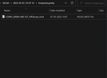
I downloaded the fablab library from here.
IMPORTING THE LIBRARIES
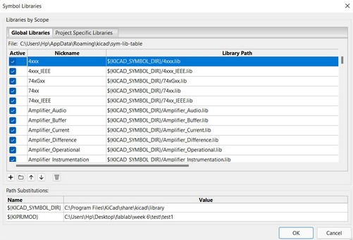
To add the fab library(fablab.lib), go to Preferences-Manage Symbol libraries.
Add the fablab.lib file.
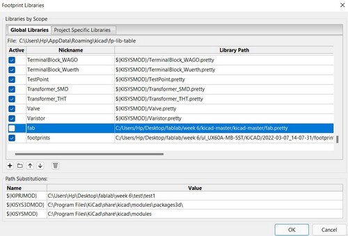
To add the footprint library(fab.pretty), go to Preferences-Manage Footprint libraries. Add the fab.pretty file.
WORKFLOW WITH KICAD
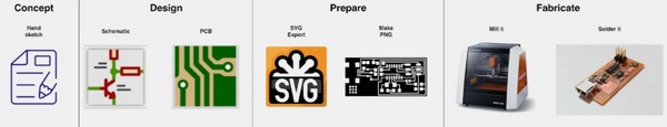
1. CONCEPT SKECTHES
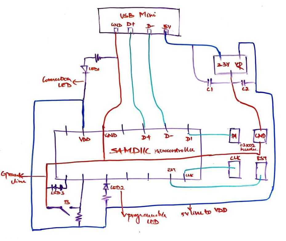
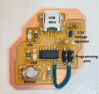
I decided on adding
- 1 LED connected to 5v which indicates connection to a computer.
- 1 LED connected to the microcontroller that can be programmed later on.
- 1 button to be programmed, connected to the microcontroller
- Mini Usb connector for durability
2. SCHEMATIC
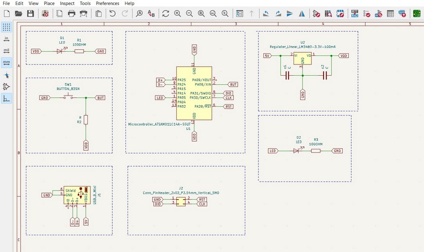
Importing new symbols through digikey
I decided to look for the digital files for the components available in our fablab inventory through DIGIKEY.. I imported both symbol and footprint library for the new component.
I realised that some the Components were missing footprints. So I had to change the name of the footprint file to match the one that software was looking for.
Eventually, I downloaded a newer version of Kicad and that fixed few of the above mentioned problems.
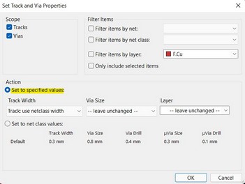
After the schematic, remember to set the trace width to 3mm.
I forgot to do it beforehand, but
I found a way to do it after drawing the traces (not recommended
).
To change the track width later:
Go to Edit-> Edit track via properties
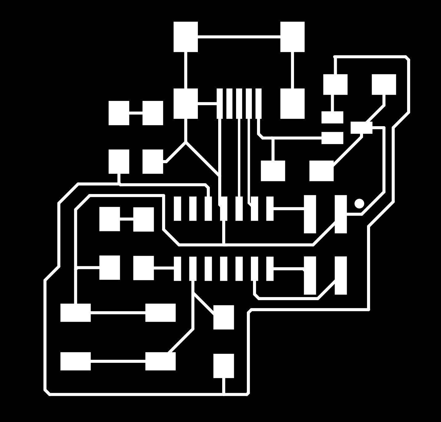
3. PCB
After setting the track width, you can start laying out the traces between components and you can then export it as an SVG.4. INKSCAPE
P> Import the SVG file into Inkscape,1. Create seperate layers for the Traces, Outline and Background.
2. Use fill and stroke to make the traces white and the background dark.
3. You can either draw the outline in inkscape or import them from Kicad.

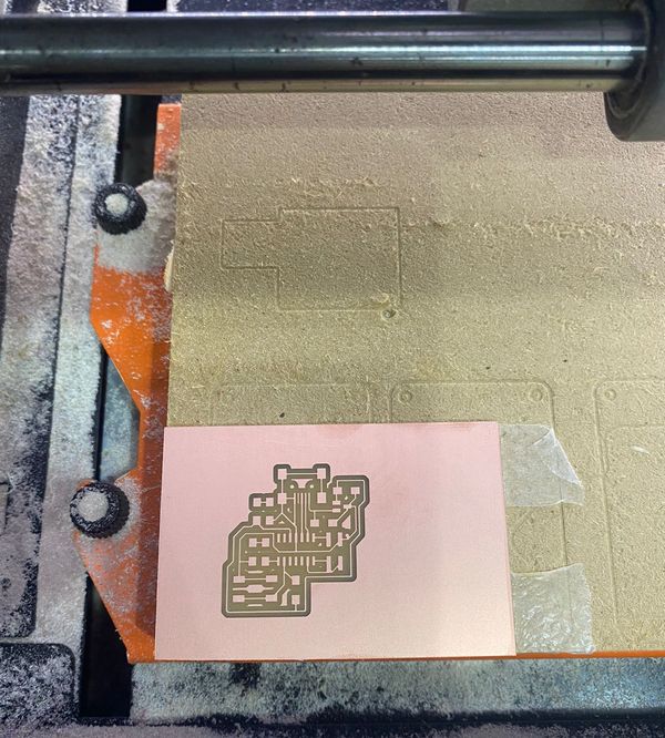
5. FABRICATING THE BOARD
MILLINGUpload the PNG file exported from Inskcape to modsproject and download the .rml file for milling. Mill the board by following the procedure from WEEK 04 documentation.
STUFFING THE BOARD
Design files download
Kicad